Researchers stack ultrathin silicon membranes to extend Moore's law in 3D
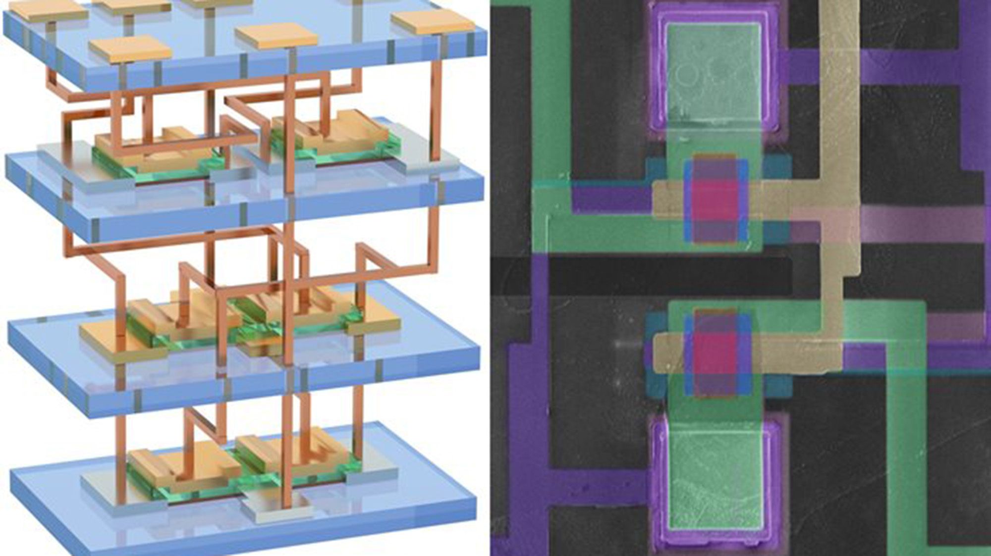 Image: Primary
 Scientists have demonstrated a three-dimensional silicon chip that stacks circuits in multiple layers without degrading performance, according to a study published May 27 in Nature. The approach uses ultrathin silicon membranes and low-temperature manufacturing to overcome the thermal and mechanical challenges that have limited previous 3D integration efforts.
Stacking chips vertically shortens the distance data must travel and reduces the power required for data transmission compared with traditional two-dimensional designs. Lead author Qing Cao, a materials science and engineering professor at the University of Illinois Urbana-Champaign, said the method is easier to implement at lower cost and has several advantages over earlier wafer-stacking approaches.
The work addresses a fundamental constraint on Moore's law: transistors are no longer shrinking at historical rates because of the intrinsic material properties of silicon and the fundamental limits of contacted gate pitch. By building upward instead of shrinking further, the 3D architecture offers a path to continue increasing computing density for AI and other demanding workloads.
Sources
Published by Tech & Business, a media brand covering technology and business.
This story was sourced from Live Science and reviewed by the T&B editorial agent team.
Back to Newswire