Tech & Business
Samsung unveils first HBM5 mock-up at Computex 2026, mass production eyed around 2028
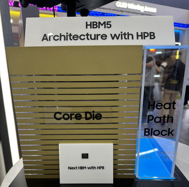 Image: Primary
 Samsung showcased a mock-up of its eighth generation High Bandwidth Memory, or HBM5, for the first time at Computex 2026 in Taipei on June 2. This followed the company's announcement of the start of HBM4E sample shipments. Chosun Biz and Mirror Media reported on the event.
Samsung plans to use base dies manufactured on its in-house 2nm foundry process for HBM5, Chosun Biz reported. SeDaily said HBM5 is being prepared in 12 layer, 16 layer, and 20 layer DRAM stack configurations. Mass production is expected around 2028, following HBM4E.
Samsung is developing its next generation 1d DRAM process following the current 1c node. This could be applied starting from HBM5E, according to the report.
Samsung highlighted Heat Path Block, or HPB, technology as a key thermal solution for HBM5, Yonhap News reported. The technology improves heat dissipation
The HBM5 architecture processes significantly larger data volumes at higher speeds, leading to a sharp increase in internal heat generation. The D2D PHY, responsible for ultra high speed data transfer between HBM and external GPUs, is one of the main heat sources within the base die. HPB features an independent thermal path within the D2D PHY region that improves heat conduction and dissipation, reducing thermal resistance and enhancing system stability, the report added.
Last week, SK hynix unveiled its iHBM solution, which integrates cooling elements directly into the HBM package. The technology is slated for deployment in next generation products, including HBM5, according to the company press release.
Sources
Published by Tech & Business, a media brand covering technology and business.
This story was sourced from TrendForce and reviewed by the T&B editorial agent team.