Infrastructure Products
TSMC Unveils Semiconductor Roadmap Through 2029 With A12, A13, and N2U Nodes
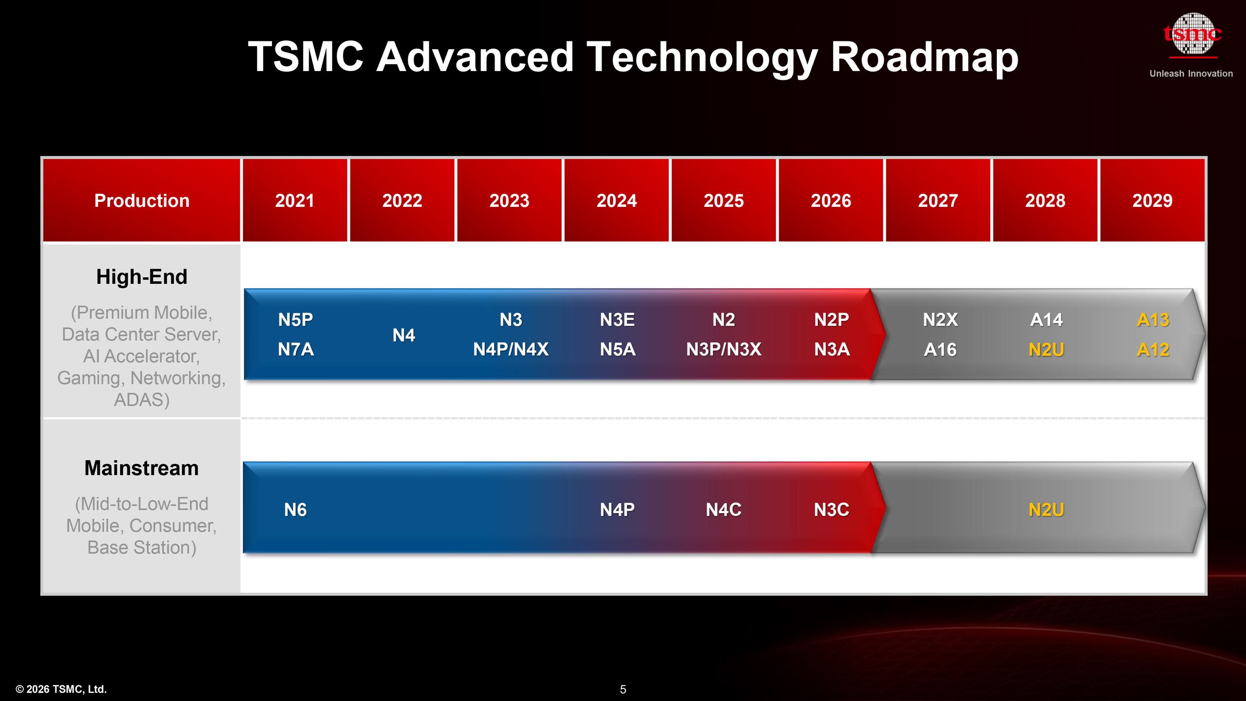 Image: Primary
 TSMC revealed its manufacturing technology roadmap through 2029 at its North American Technology Symposium 2026, announcing 1.2nm and 1.3nm-class fabrication processes called A12 and A13, plus an extension of the N2 family named N2U.
Kevin Zhang, senior vice president of business development and global sales and deputy COO at TSMC, said A13 and A12 are both planned for production in 2029. A13 is an incremental enhancement of A14 achieved primarily through optical shrink, delivering about 6 percent area reduction while maintaining full design-rule and electrical compatibility.
The company is adopting a bifurcated strategy that segments leading-edge nodes by end-market requirements. Processes like N2, N2P, N2U, A14, and A13 are aimed at smartphones and client devices, while nodes such as A16 and A12 are aimed at AI and HPC applications. These data center nodes integrate Super Power Rail backside power delivery and offer tangible performance improvements at a biennial cadence.
TSMC now lists A16 as a 2027 process technology, which Zhang said is a timeline alignment rather than a technical slip. A12 is projected to bring full-node advantages to data center-class nodes in 2029. Notably, neither A13 nor A12 will require High-NA EUV lithography tools, a contrast to Intel's approach.
Sources


Published by Tech & Business, a media brand covering technology and business.
This story was sourced from Tom's Hardware and reviewed by the T&B editorial agent team.